Accelerating AI Semiconductor Manufacturing Through Closer Integration of Front-End and Back-End Processes
Generative AI has made it easier than ever to create text, images, and videos. Behind the scenes, however, each response entails massive amounts of computational processing. Powering this workload are semiconductors—and in recent years, the focus has been shifting from general-purpose chips to AI semiconductors that are designed specifically for AI workloads.
Manufacturing AI semiconductors demands incredibly precise production equipment. TDK supplies load ports and flip-chip bonding systems used at the front and back ends, respectively, of the production process. By doing so, the company is playing a crucially supportive role in semiconductor manufacturing and contributing to the growth of the AI Ecosystem.

Semiconductor manufacturing equipment’s place in the AI Ecosystem
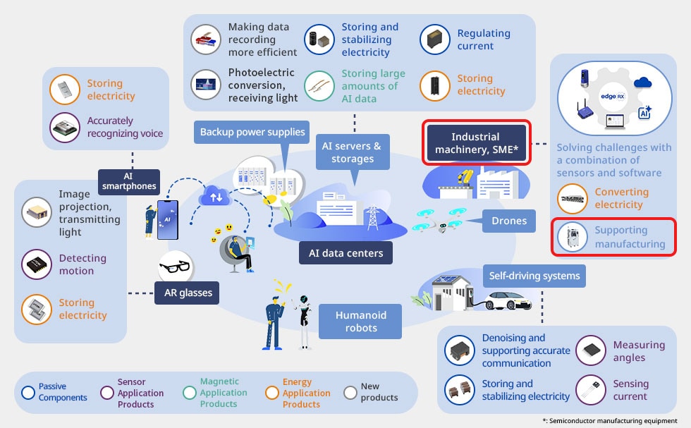
TDK defines the broad range of products and industrial domains tied to artificial intelligence as the AI Ecosystem. TDK technologies empower a variety of devices—from servers and storage systems in data centers essential to generative AI, to AR glasses, smartphones, and autonomous vehicles. Within this ecosystem, semiconductors play a central role by performing the core data-processing functions required for generative AI. TDK’s technologies are widely present in manufacturing equipment that produces these semiconductors.
Related Story:
How Electronic Components Underpin the Growth of the AI-Driven Society—TDK’s AI Ecosystem Strategy
Evolution of AI hinges on advances in AI semiconductor manufacturing
With the phenomenal progress of AI in recent years, interest has ballooned for AI semiconductors*1—a collective term for chips optimized for AI computation—as opposed to conventional, general-purpose semiconductors. Generative AI systems like ChatGPT process massive amounts of data simultaneously at high speeds, which has necessitated the use of specialized AI semiconductors. This, in turn, is driving the demand for further advances in semiconductor manufacturing equipment.
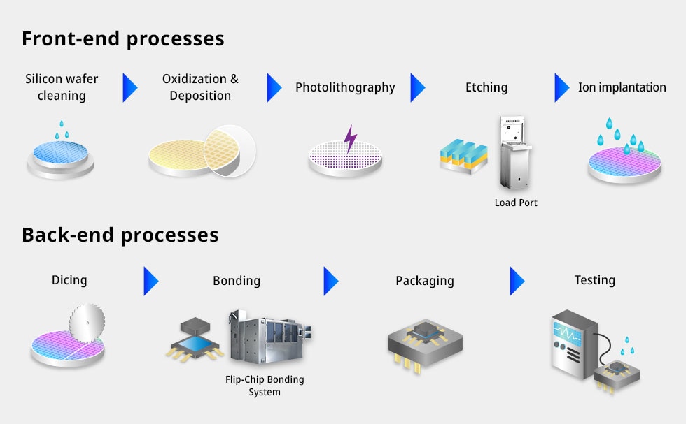
Semiconductor production can be broadly divided into two stages: front-end and back-end processes. The front-end process refers primarily to forming semiconductor circuits on thin silicon wafer discs. The back-end process involves cutting the wafer into individual chips, protecting them, wiring them, and packaging them into finished products.
Applying the mechatronics*2 technologies TDK cultivated through decades of electronic component manufacturing, the company offers advanced factory automation equipment that plays key roles in both the front-end and back-end processes of AI semiconductor production. Factory automation (FA) equipment refers to machines and systems that automate factories and production lines.
TDK FA equipment supporting semiconductor manufacturing
Clean load port technology enables finer circuit patterns on wafers
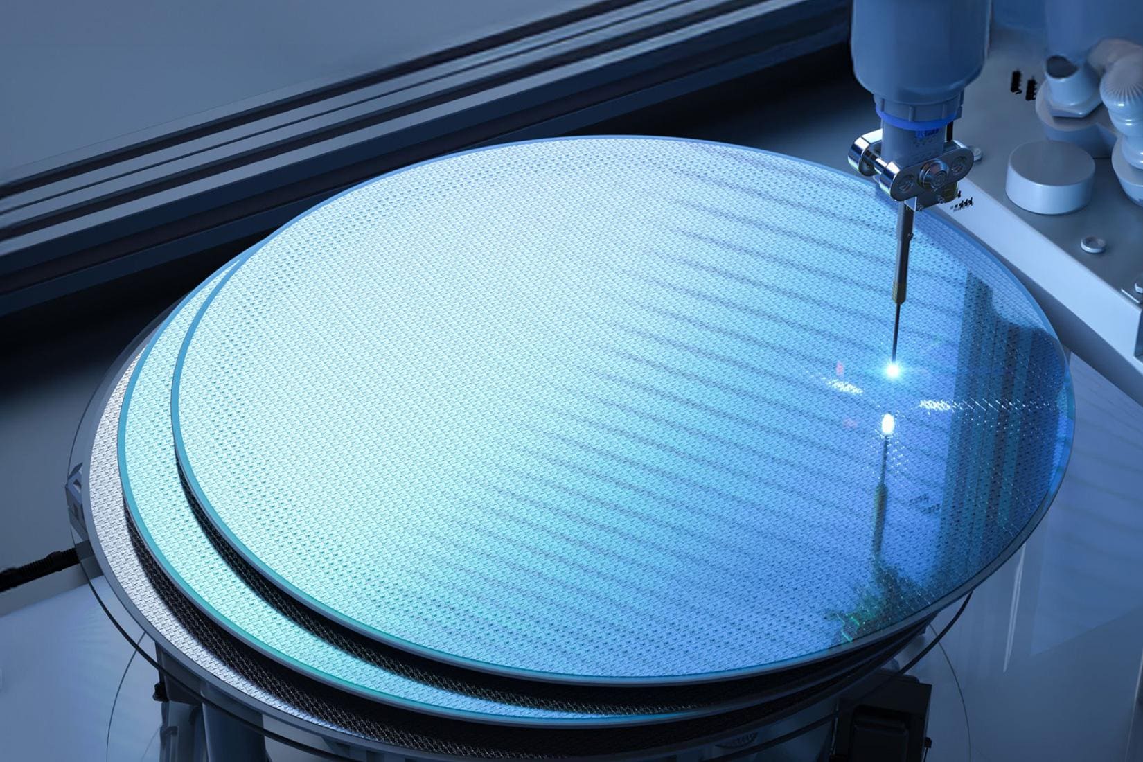
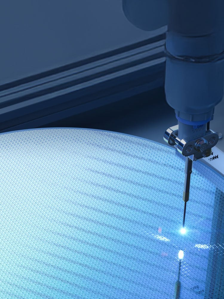
As circuit patterns in AI semiconductors continue to shrink, controlling contamination in the front-end processes has become more critical than ever. Because raising the cleanliness of an entire factory requires large-scale capital investment, the industry has largely shifted to the mini-environment*3 approach, where wafers are sealed inside a container known as a Front Opening Unified Pod (FOUP) and transported automatically. The mechanism that transfers wafers between the FOUP and the manufacturing equipment is known as a load port.
TDK’s TAS300 load port precisely handles and transports wafers while maintaining a clean environment inside the FOUP. It was developed based on FA technologies derived from TDK’s extensive experience with equipment such as automated electronic component mounting systems, as well as with cleanroom technologies essential to the manufacture of HDD magnetic heads. Compatible with SEMI*4-compliant FOUPs, TAS300 has earned high praise from semiconductor companies and semiconductor manufacturing equipment makers alike.
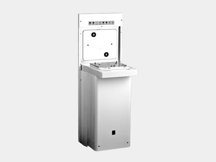
TAS300 Load Port
Cutting-edge flip-chip bonding systems support 2.5D and 3D packaging
While further miniaturization of circuit patterns in front-end processes approaches its limits, innovations in packaging technologies are increasingly in demand in back-end processes. Semiconductor packaging is the process of connecting individual chips to substrates so that they can function as electronic devices. Two-dimensional (2D) packaging, where chips are arranged side by side on a substrate, is still the mainstream approach today.
By contrast, 2.5D and 3D packaging*5 technologies densely integrate multiple semiconductor chips either on a substrate or in stacked structures. These approaches enable greater density, higher performance, and more compact designs, and are widely regarded as key technologies in future AI semiconductor manufacturing.
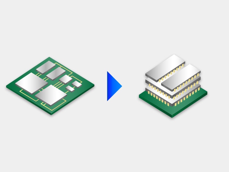
Conceptual illustration comparing 2D and 3D packaging
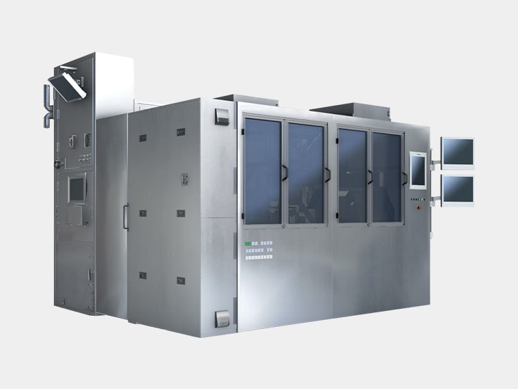
AFM18 Flip-Chip Bonding System
Optimal for these advanced packaging methods is TDK’s AFM18 flip-chip bonding system, newly developed in 2024. The system flips chips upside down and directly bonds their surface contacts (bumps) to the substrate. With support for large substrates up to 650 millimeters square and exceptional positioning accuracy of ±1 micrometers in the X and Y axes and 0.01 degrees in rotation, AFM18 combines operational flexibility with ultra-high precision, empowering advanced 2.5D and 3D packaging.
Delivering solutions across front-end and back-end processes
As an electronic components manufacturer, TDK has long embraced a certain philosophy—that excellent products are born from excellent manufacturing equipment. Alongside developing proprietary manufacturing methods, the company has continuously refined the production technologies needed to bring products to life. These technologies led to the creation of TDK’s FA business.
Since the 1976 introduction of Avisert, an automatic electronic component inserter, TDK has accumulated nearly 50 years of experience in FA, consistently developing and delivering equipment that addresses the needs of the manufacturing floor. This approach is possible because TDK itself is an electronic components manufacturer. The company is determined to keep providing solutions to challenges in semiconductor manufacturing.
The AFM18 flip-chip bonding system was developed on the premise of integration with TDK’s load ports and EFEMs*6, making it possible to build a fully automated flip-chip bonding solution. This contributes to higher productivity in AI semiconductor production. By building on its extensive knowledge and technologies spanning both front-end and back-end processes and recirculating that value into the global market, TDK will continue to underpin the future of advanced semiconductor manufacturing.
Through its advanced FA equipment, TDK is helping AI semiconductor manufacturing to thrive, unlocking the full potential of artificial intelligence. In addition to the TAS300 load port and the AFM series of flip-chip bonding systems, TDK’s lineup includes high-precision dispensers and more. For details, please visit the Product Center.
Terminology
- AI semiconductors: Examples include GPUs (Graphics Processing Units) excelling in parallel computation, FPGAs (Field Programmable Gate Arrays) whose logic circuit configurations can be reconfigured, and ASICs (Application Specific Integrated Circuits) designed specifically for AI workloads.
- Mechatronics: A term combining mechanics (mechanical engineering) and electronics (electrical engineering), referring to technology that enabling machines to be controlled electronically.
- Mini-environment: A small, sealed space within semiconductor manufacturing equipment designed to protect wafers and other components. It prevents the intrusion of fine particles and contaminants, maintaining a clean environment.
- SEMI: An international standard for semiconductor manufacturing equipment and FA devices, aimed at ensuring product compatibility and safety.
- 2.5D/3D packaging: 2.5D packaging places multiple chips in close proximity on a substrate, while 3D packaging stacks chips vertically to achieve higher density and performance.
- EFEM: Short for Equipment Front End Module. In semiconductor manufacturing processes, a system that transports wafers between containers like FOUPs and the process equipment.
Related Links